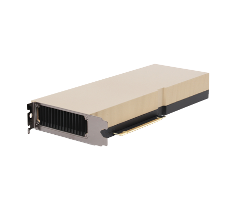
Optimized for large language model inference, the NVIDIA H100 NVL GPU combines Hopper architecture with 94GB of HBM3 memory in a PCIe form factor. This dual-slot, 10.5-inch PCIe Gen5 card supports up to 3x NVIDIA NVLink bridges, allowing a pair of cards to connect with 600 GB/s of bidirectional bandwidth and deliver a combined 188GB of shared memory. Designed for demanding AI workloads rather than gaming, the H100 NVL does not include display connectivity.
Featuring a PCIe 5.0 x16 interface, the full-height, full-length, double-width NVIDIA H100 NVL utilizes a passive heat sink for cooling and operates at a maximum thermal design power (TDP) of up to 400W through a single 16-pin power connector. In addition, it incorporates second-generation Multi-Instance GPU (MIG) technology, which partitions the GPU into up to 7x isolated instances of 12GB each. NVIDIA AI Enterprise is also included.
For NVIDIA-Certified systems, the H100 NVL operates at a base clock speed of 1,080 MHz and a boost clock speed of 1,785 MHz. Its powerful Tensor Cores deliver peak performance of up to 3,341 TFLOPS for FP8 operations and 1,671 TFLOPS for FP16/BFLOAT16 operations, making it a powerful solution for AI inference and other computationally intensive workloads.
If you know what you want but can't find the exact configuration you're looking for, have one of our knowledgeable sales staff contact you. Give us a list of the components you would like to incorporate into the system, and the quantities, if more than one. We will get back to you immediately with an official quote.
Your privacy is our priority. We use cookies to offer an improved online experience.
By clicking 'Accept all', you consent to our use of all cookies. You may click
'Configure settings' to only enable the specific categories you have chosen below.
To manage broader privacy rights or opt out of data sharing, visit our
Your Privacy Choices page.
Cookie Settings
IT Creations uses three primary categories of cookies as described below. You can decide
which categories of cookies you wish to accept to improve your experience on our website.
To learn more about the specific cookies we use on our site and how they impact your
experience, please read our
Cookie Policy.
Global Privacy Control (GPC)
We automatically respect browser-based Global Privacy Control signals.
Current GPC signal status:
Enabled
If GPC is enabled, we automatically disable the sale or sharing of your personal data for this browser.
Default Cookies
These cookies are necessary to ensure the proper functioning of the website.
They enable core functionality such as security, network management, and
accessibility. Without these, the website cannot function correctly.
Analytics Cookies
These cookies help us understand how visitors interact with our website by
collecting and reporting information anonymously. This data allows us to
improve our website's performance and provide a smoother user experience.
Marketing Cookies
These cookies are used to track visitors across websites. The intention is
to display ads that are relevant and engaging for the individual user and
thereby more valuable for publishers and third-party advertisers.
Consult the Experts!Talk to one of our trained professionals to create a system to your exact specifications.

 Additional Information